
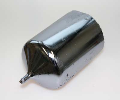
Gallium arsenide (GaAs) single crystal
|
Major capability parameter
|
|||||||
|
Single crystal
|
Doped
|
Conduction type
|
Carrier concentration
(/cm3) |
EPD
(/cm2)
|
Growth method
|
Wafer size
|
|
|
GaAs wafer
|
Un-doped
|
Semi-insulating |
/
|
<5x10⁵
|
LEC
HB
|
φ6"x0.625mm
φ4"x0.6mm
φ2"x0.35mm
|
|
|
Si-doped
|
N-type
|
>5×10¹⁷
|
|||||
|
Cr-doped
|
Si-type
|
/
|
|||||
|
Fe-doped
|
N-type
|
~2×10¹⁸
|
|||||
|
Zn-doped
|
P-type
|
>5×10¹⁷
|
|||||
|
Orientation
|
<100>, <111>, or other off-angle orientation
|
||||||
|
Standard Size(mm)
|
φ2"x0.35mm, φ3"x0.6mm, φ4"x0.625mm, φ6"x0.625mm,
25x25x0.5mm, 10x10x0.5mm, 10x5x0.5mm, 5x5x0.5mm
Special size and orientation are available upon request
|
||||||
|
Surface roughness
|
(Ra):<=5A(0.5nm)
|
||||||
|
Polishing
|
Single side polished or Double side polished
|
||||||
|
Packing
|
100 clean bag,1000 exactly clean bag
|
||||||
We supply Gallium arsenide (GaAs) crystal , Gallium arsenide semiconductor crystals material. Welcome to order various sizes and specifications of GaAs single crystal.
Contact Us
- BIOTAIN CRYSTAL CO., LIMITED
- Tel: (+86) 1506 0796 451
- Fax: (+86) 0597 2212602
- Email: sales@crystal-material.com
- Work Time ( GMT +8 ):
- 9 AM ~ 6 PM, Monday to Friday
- Main office: A7, No. 501, Denggaoxi Road, Xipi street, Xinluo District, Longyan, Fujian, China
Products Category
- Substrate Materials
- Single crystal substrates
- Optical windows
- Conductive glass
- Ceramic substrates
- Single Crystals
- Sputtering Targets
- Compound Ceramic Target
- Alloy targets
- High purity Metal targets
- Evaporation material
- Oxides materials
- Fluorides materials
- Metal materials
- Nitride, Sulfide and Selenide
- High purity Nano powders