
BIOTAIN CRYSTAL > Substrate Materials > Single crystal substrates > Product Information > Next :GaN on Sapphire wafer
GaN on Silicon wafer
|
Standard Specification |
|
|
ITEM |
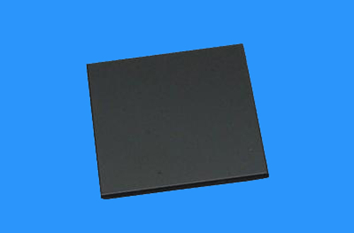
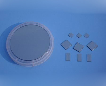
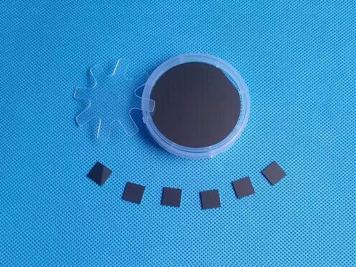
Gallium Nitride on Silicon wafer, GaN on Silicon wafer |
|
GaN thin film |
0.5μm ± 0.1 μm |
|
GaN orientation |
C-plane (0001) |
|
Ga-face |
<1nm, As-grown, EPI-ready |
|
N-face |
P-type/B-doped |
|
Polarity |
Ga-face |
|
Conductivity type |
Undoped/N-type |
|
Macro defect density |
<5/cm^2 |
|
|
|
|
Silicon wafer substrate |
|
|
Orientation |
<100> |
|
Conductivity type |
N-type/P-doped or P-type/B-doped |
|
Dimension: |
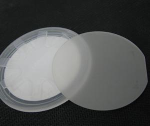
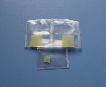
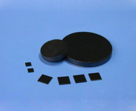
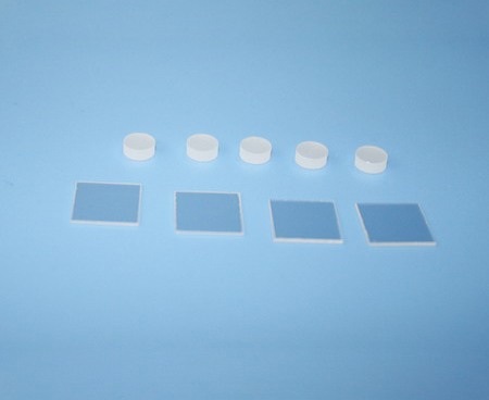
10 x 10 x 0.5mm, Single side polished |
|
Resistivity |
1-5 ohm-cm, 0-10 ohm-cm, <0.005 ohm-cm or others |
The GaN on Silicon wafer is to deposite a GaN thin film layer on semiconductor silicon wafer, by use this method to reduce costs and to replace Gallium Nitride single crystal substrate.
We can customize the GaN on Silicon wafer upon customer's requirements,
Contact Us
- BIOTAIN CRYSTAL CO., LIMITED
- Tel: (+86) 1506 0796 451
- Fax: (+86) 0597 2212602
- Email: sales@crystal-material.com
- Work Time ( GMT +8 ):
- 9 AM ~ 6 PM, Monday to Friday
- Main office: A7, No. 501, Denggaoxi Road, Xipi street, Xinluo District, Longyan, Fujian, China
Products Category
- Substrate Materials
- Single crystal substrates
- Optical windows
- Conductive glass
- Ceramic substrates
- Single Crystals
- Sputtering Targets
- Compound Ceramic Target
- Alloy targets
- High purity Metal targets
- Evaporation material
- Oxides materials
- Fluorides materials
- Metal materials
- Nitride, Sulfide and Selenide
- High purity Nano powders