
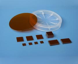
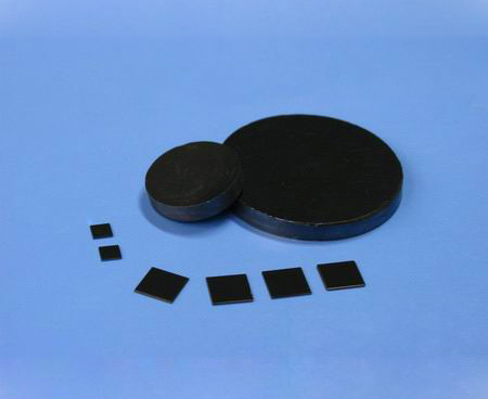
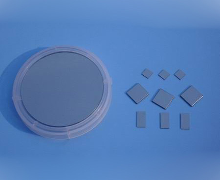
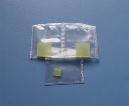
GaP substrate
|
Substrate material |
Single crystal Gallium Phosphide (GaP) |
|
Crystal structure |
Cubic a =5.4505 Å |
|
Growth method |
Czochralski (CZ) |
|
Density: |
4.13 g/cm3 |
|
Melting point: |
1480 ℃ |
|
Coefficient of thermal expansion: |
5.3 x10⁻⁶ |
|
Doping: |
S-doped/N-type; Undoped/N-type |
|
Thermal conductivity: |
2~8 x10¹⁷/cm3; 4~ 6 x10¹⁶/cm3 |
|
Resistivity (W.cm) |
~0.03; ~0.3 |
|
EPD (cm-2 ): |
< 3x10E5; < 3x10E5 |
|
Standard Orientation |
<111> or <100> |
|
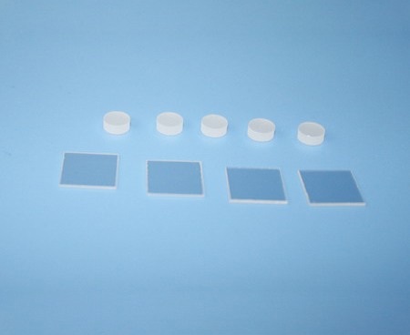
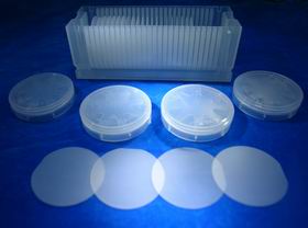
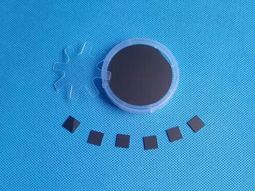
Standard size |
10x10x0.5mm, Dia2"x0.5mm, Dia2"x0.28mm |
|
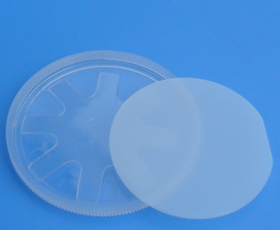
Polishing |
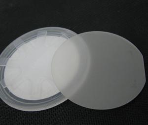
Single side polished or Double side polished |
The crystal structure of Gallium Phosphide(GaP) is a sphalerite type, which is an indirect transition type semiconductor. It is one of the main substrate materials for LEDs.
The Gallium Phosphide(GaP) epitaxial material is obtained by liquid-phase epitaxy or vapor-phase epitaxy and diffusion growth on a gallium phosphide single crystal substrate. The GaP is mostly used to manufacture light-emitting diodes. The GaP liquid-phase epitaxial material can produce red, green, yellow-green light-emitting diodes. And the GaP Vapor-phase epitaxial and diffusion-grown material can produce yellow, yellow-green light-emitting diodes.
Contact Us
- BIOTAIN CRYSTAL CO., LIMITED
- Tel: (+86) 1506 0796 451
- Fax: (+86) 0597 2212602
- Email: sales@crystal-material.com
- Work Time ( GMT +8 ):
- 9 AM ~ 6 PM, Monday to Friday
- Main office: A7, No. 501, Denggaoxi Road, Xipi street, Xinluo District, Longyan, Fujian, China
Products Category
- Substrate Materials
- Single crystal substrates
- Optical windows
- Conductive glass
- Ceramic substrates
- Single Crystals
- Sputtering Targets
- Compound Ceramic Target
- Alloy targets
- High purity Metal targets
- Evaporation material
- Oxides materials
- Fluorides materials
- Metal materials
- Nitride, Sulfide and Selenide
- High purity Nano powders