
BIOTAIN CRYSTAL > Substrate Materials > Single crystal substrates > Product Information > Next :GaN on Silicon wafer
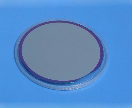
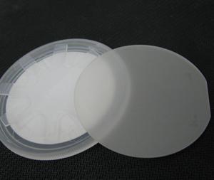
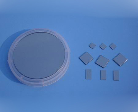
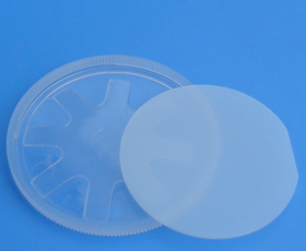
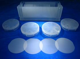
SOI wafer
|
Silicon-On-Insulator (SOI) wafer |
|
|
Structure |
Si + SiO2 + Si |
|
Standard Diameter |
4-inch(100mm), 6-inch(150mm), 8-inch(200mm) |
|
Orientation |
<100> |
|
Type/Dopant |
P-type/B-doped, N-type/P-doped |
|
Handle wafer thickness |
400um, 675um, 725um |
|
Resistivity |
1~20 ohm-cm, 1~100 ohm-cm, 0.001~0.005 ohm-cm or others |
|
|
|
|
Buried Oxide layer |
500nm, 1um, 2um, 3um |
|
|
|
|
Device layer |
70nm, 220nm, 340nm, 2um, 10um, 30um, 80um |
|
Orientation |
<100> |
|
Type/Dopant |
P-type/B-doped, N-type/P-doped, |
|
Resistivity |
1~20 ohm-cm, 1~100 ohm-cm, 0.001~0.005 ohm-cm or others |
SOI wafer is mean the Silicon-On-Insulator wafer which is silicon on an insulating substrate (Si + SiO2 + Si), and a buried oxide layer is introduced between the top silicon and the back substrate.
By forming a semiconductor thin film on an insulator, SOI wafer materials have advantages that are incomparable to bulk silicon: It can realize the dielectric isolation of components in integrated circuits, completely eliminating the parasitic latch-up effect in bulk silicon CMOS circuits. The integrated circuit made of SOI also has the advantages of small parasitic capacitance, high integration density, high speed, simple process, smaller short channel effect, and especially suitable for low voltage and low power circuits. SOI will become the mainstream technology for deep submicron low voltage, low power integrated circuits. In addition, SOI materials are also used to fabricate MEMS optical switches,
SOI advantages:
1) Reduced parasitic capacitance and increased operating speed. Compared to bulk silicon materials, SOI devices operate at speeds of 20-35%;
2) has lower power consumption. SOI device power consumption can be reduced by 35-70% due to reduced parasitic capacitance and reduced leakage;
3) Eliminate the latch-up effect;
4) suppressing the pulse current interference of the substrate and reducing the occurrence of soft errors;
5) Compatible with existing silicon processes to reduce processes by 13-20%.
Contact Us
- BIOTAIN CRYSTAL CO., LIMITED
- Tel: (+86) 1506 0796 451
- Fax: (+86) 0597 2212602
- Email: sales@crystal-material.com
- Work Time ( GMT +8 ):
- 9 AM ~ 6 PM, Monday to Friday
- Main office: A7, No. 501, Denggaoxi Road, Xipi street, Xinluo District, Longyan, Fujian, China
Products Category
- Substrate Materials
- Single crystal substrates
- Optical windows
- Conductive glass
- Ceramic substrates
- Single Crystals
- Sputtering Targets
- Compound Ceramic Target
- Alloy targets
- High purity Metal targets
- Evaporation material
- Oxides materials
- Fluorides materials
- Metal materials
- Nitride, Sulfide and Selenide
- High purity Nano powders