
BIOTAIN CRYSTAL > Substrate Materials > Single crystal substrates > Product Information > Next :NaCl substrate
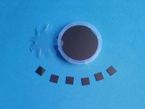
Silicon wafer/substrate
Click here for: Thermal oxide Silicon wafer (SiO2 + Si)
Click here for: Silicon-On-Insulator, SOI wafer (Si+ SiO2 + Si)
|
The main performance parameter
|
|||
|
Crystal Structure
|
Cubic
|
||
|
Melting point(℃)
|
1420
|
||
|
Density
|
2.4(g/cm3)
|
||
|
Growth method
|
Float Zone (FZ)
Czochralski (CZ) magnetic field Czochralski method (MCZ) |
||
|
Dopant
|
Un-doped
|
Boron-doped
|
Phos-doped / As-doped
|
|
Conductivity Type
|
Intrinsic
|
P-type
|
N-type
|
|
Resistivity
|
>1000 Ω-cm
>10000 Ω-cm |
0.001~0.005 Ω-cm
0.01~0.09 Ω-cm 0.1~0.9 Ω-cm 1~10 Ω-cm 20~100 Ω-cm |
0.001~0.005 Ω-cm 0.01~0.09 Ω-cm 0.1~0.9 Ω-cm 1~10 Ω-cm 20~100 Ω-cm |
|
EPD
|
/
|
/
|
/
|
|
Oxygen Content(/cm3)
|
≤8x10¹⁷
|
≤8x10¹⁷
|
≤8x10¹⁷
|
|
Carbon Content(/cm3)
|
≤5x10¹⁶
|
≤5x10¹⁶
|
≤5x10¹⁶
|
|
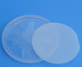
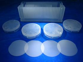
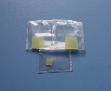
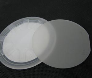
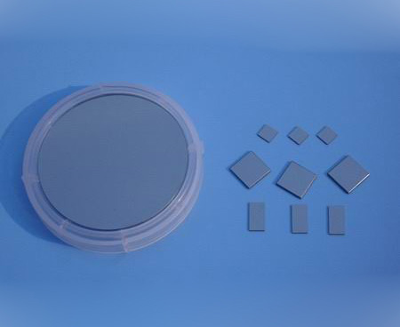
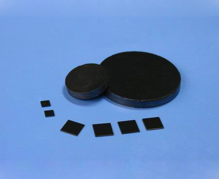
Packing
|
Class-100 clean bag, class-1000 clean room
|
||
|
Special specification
|
We can customize Specific spcification upon requirements
|
||
| Standard Specification | |||||
| Product Name | Orientation | Standard Size | Thickness | Polishing | |
|
Silicon substrate/wafer (Un-doped or P-type or N-type) |
<100> ±0.5° <110> ±0.5° <111> ±0.5° <211> ±0.5° Or other off-angle |
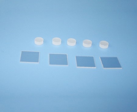
10x10mm 10x5mm 5x5mm 20x20mm φ2" x 0.28mm φ3" x 0.38mm φ4" x 0.5mm φ6" x 0.625mm φ8" x 0.725mm φ12" x 0.775mm Or others |
0.1mm 0.2mm 0.28mm 0.38mm 0.5mm 0.525mm 0.625mm 1.0mm ±25μm Or others |
Fine ground Single side polished Double side polished Roughness: Ra<10A(1.0nm) Roughness: Ra<5A(0.5nm) |
Inquiry Online |
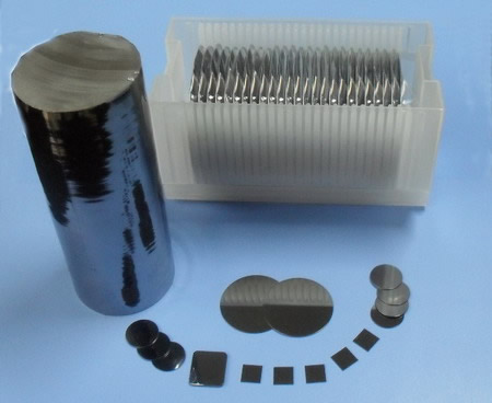
Silicon wafer can be used in the production and deep processing of diodes, rectifier devices, circuits, and solar cell products. Its subsequent product integrated circuits and semiconductor separation devices have been widely used in various fields, and also occupy an important position in military electronic equipment.
Silicon wafer for manufacturing semiconductor Silicon devices for high power rectifiers, high power transistors, diodes, switching devices, and the like. It is a promising material in the development of energy. The growth methods of single crystal Silicon include Czochralski method (CZ), Floating Zone method (FZ), and epitaxial method. The Czochralski Monocrystalline Silicon wafer is mainly used for a semiconductor integrated circuit, a diode, an epitaxial wafer substrate, and a solar cell.
Contact Us
- BIOTAIN CRYSTAL CO., LIMITED
- Tel: (+86) 1506 0796 451
- Fax: (+86) 0597 2212602
- Email: sales@crystal-material.com
- Work Time ( GMT +8 ):
- 9 AM ~ 6 PM, Monday to Friday
- Main office: A7, No. 501, Denggaoxi Road, Xipi street, Xinluo District, Longyan, Fujian, China
Products Category
- Substrate Materials
- Single crystal substrates
- Optical windows
- Conductive glass
- Ceramic substrates
- Single Crystals
- Sputtering Targets
- Compound Ceramic Target
- Alloy targets
- High purity Metal targets
- Evaporation material
- Oxides materials
- Fluorides materials
- Metal materials
- Nitride, Sulfide and Selenide
- High purity Nano powders