
BIOTAIN CRYSTAL > Single Crystals > Product Information > Next :Bismuth germanate (BGO) single crystal
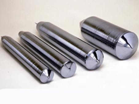
Silicon (Si) single crystal
|
Major capability parameter
|
|||
| Growth method | Czochralski(CZ), floating zone(FZ) | ||
| Crystal structure | Cubic | ||
| Band gap | 1.12 eV | ||
| Density | 2.4 g/cm3 | ||
| Melting point | 1420℃ | ||
| Dopant type | Undoped | Boron-doped | Phos-doped / As-doped |
| ConductiveType | Intrinsic | P-type | N-type |
| Resistivity | >1000 Ωcm | 0.001~100 Ωcm | 0.001~100 Ωcm |
| EPD | <100 /cm2 | <100/cm2 | <100/cm2 |
| Oxygen content | ≤1x10¹⁸ /cm3 | ||
| Carbon content | ≤5x10¹⁶ /cm3 | ||
| Standard Size | 5x5mm, 10x5mm, 10x10mm, 15x15mm, 20x15mm, 20x20mm | ||
| φ2”x0.28mm, φ3” x 0.38mm, φ4” x 0.5mm, φ6” x 0.625mm, φ8” x 0.725mm, 10x10mm | |||
| Thickness | 0.1mm, 0.28mm, 0.5mm, 1.0mm or others | ||
| Polishing | Single side polished or Double side polished | ||
| Crystal orientation | <100>, <110>, <111> ±0.5º or other off-angle | ||
| Surface roughness | Ra≤5Å(5µmx5µm) | ||
| Packing | 100 clean bag,1000 exactly clean bag | ||
We supply Silicon (Si) single crystal , Silicon semiconductor crystals material. used as semiconductor materials, high-power transistors, rectifiers, solar cells. Welcome to order various sizes and specifications of Silicon single crystal.
Our Silicon single crystal is growth by the methods of Czochralski (CZ) and Floating Zone (FZ), and epitaxial method. The Czochralski method Silicon single crystal is mainly used for a semiconductor integrated circuit, a diode, epitaxial wafer, and solar cell.
Contact Us
- BIOTAIN CRYSTAL CO., LIMITED
- Tel: (+86) 1506 0796 451
- Fax: (+86) 0597 2212602
- Email: sales@crystal-material.com
- Work Time ( GMT +8 ):
- 9 AM ~ 6 PM, Monday to Friday
- Main office: A7, No. 501, Denggaoxi Road, Xipi street, Xinluo District, Longyan, Fujian, China
Products Category
- Substrate Materials
- Single crystal substrates
- Optical windows
- Conductive glass
- Ceramic substrates
- Single Crystals
- Sputtering Targets
- Compound Ceramic Target
- Alloy targets
- High purity Metal targets
- Evaporation material
- Oxides materials
- Fluorides materials
- Metal materials
- Nitride, Sulfide and Selenide