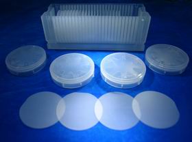
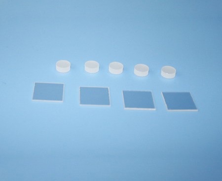
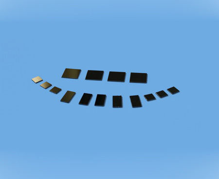
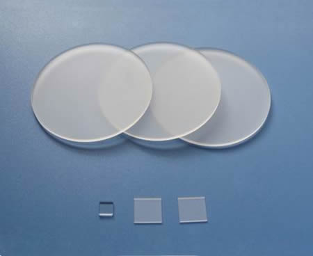
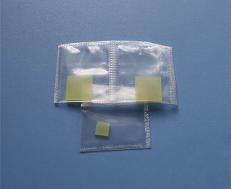
GaN substrate
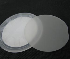
| GaN single crystal substrate/wafer | ||||
| Grade | S-level | A-level | B-level | C-level |
| Standard Size | 5X5.5mm, 10x10.5mm, 14x15mm, φ50.8mm, φ100mm | |||
| Standard Thickness | 350 ± 20 μm; 500 ± 20 μm | |||
| Marco Defect Density | <0 /cm2 | <0.3 /cm2 | <1 /cm2 | <4 /cm2 |
| Orientation | C-plane <0001> ± 0.5º | |||
|
Primary Orientation flat Second Orientation flat |
<1-100> ± 0.5°, 16mm(2-inch) / 30mm(4-inch)
<11-20> ± 3°, 8mm(2-inch) / 15mm(4-inch)
|
|||
| TTV | <= 15 μm | |||
| BOW | <= 20 μm | |||
| Dopant / Conductive |
Undoped/N-type (Resistivity: < 0.5 Ω-cm) Semi-insulating/Fe-doped (Resistivity: > 10E6 Ω-cm) Si-doped/N-type (Resistivity: < 0.05 Ω-cm ) |
|||
| Dislocation Density | <3x106 cm-2 | <3x106 cm-2 | <3x106 cm-2 | |
| Useable surface area | >90% | >80% | >70% | |
| Max size of macro defects | < 700 μm | < 2000 μm | < 4000 μm | |
| Polishing |
Ga-face surface roughness: Ra <0.3nm (Epitaxy-ready) N-face surface roughness: Ra 0.5 ~1.5 μm (optional: Ra <0.3 nm (polished)) |
|||
| Packing | Each piece individual packed in one bag, with class-100 clean bag | |||
Gallium nitride, GaN substrate. GaN has a wide direct bandgap, strong atomic bonds and high thermal conductivity, etc., and it is a strong ability on anti-radiation, Not only is the short-wavelength optoelectronic materials, Also the replacement materials of high temperature semiconductor device, GaN can be used to make blue and green LED, or violet, ultraviolet light LD, ultraviolet detectors and high-frequency high-power electronic devices.
Contact Us
- BIOTAIN CRYSTAL CO., LIMITED
- Tel: (+86) 1506 0796 451
- Fax: (+86) 0597 2212602
- Email: sales@crystal-material.com
- Work Time ( GMT +8 ):
- 9 AM ~ 6 PM, Monday to Friday
- Main office: A7, No. 501, Denggaoxi Road, Xipi street, Xinluo District, Longyan, Fujian, China
Products Category
- Substrate Materials
- Single crystal substrates
- Optical windows
- Conductive glass
- Ceramic substrates
- Single Crystals
- Sputtering Targets
- Compound Ceramic Target
- Alloy targets
- High purity Metal targets
- Evaporation material
- Oxides materials
- Fluorides materials
- Metal materials
- Nitride, Sulfide and Selenide


