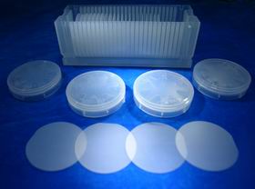
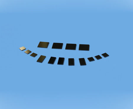
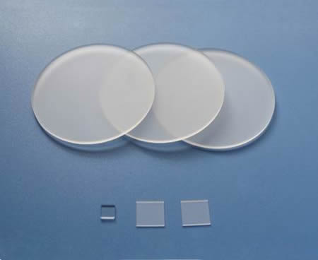
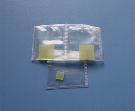
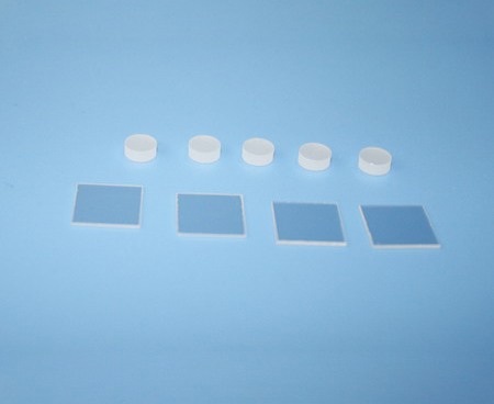
Thermal oxide Silicon wafer

|
Standard Specifications |
|
|
Product Name |
Thermal oxide Silicon wafer (SiO2/Si) |
|
|
|
|
Oxide-layer(SiO2 layer) |
25nm, 50nm, 100nm, 300nm, 500nm, 1um or others |
|
Oxidation surface |
Single-sided oxidation, Double-sided oxidation
|
|
Oxidation process |
Dry oxidation, Wet oxidation, |
|
|
|
|
Conductivity type/Dopant |
N-type/Phos-doped or N-type/As-doped or P-type/Boron-doped or Un-doped |
|
Orientation |
<100> or <111> |
|
Diameter of Silicon wafer |
2"(50.8mm), 3"(76.2mm), 4"(100mm), 6"(150mm), 8"(200mm), 12"(250mm) |
|
Thickness of Silicon wafer |
280um, 380um, 525um, 675um, 725um |
|
Resistivity (Ohm-cm) |
0.001~0.005, 0.01~0.09, 0.1~0.9, 1~10, 20~30, >100, >1000, >10000 |
|
Polishing |
Single side polished or Double side polished |
|
Surface Roughness |
Ra<5A (0.5nm) or Ra<10A (1.0nm) |
The Thermal oxide Silicon wafer is growth an oxide layer(SiO2) on Silicon wafer, also name as "SiO2 + Si wafer". Growth a good quality oxide layer on the surface of Silicon wafer is important to the entire semiconductor integrated circuit fabrication process.
Contact Us
- BIOTAIN CRYSTAL CO., LIMITED
- Tel: (+86) 1506 0796 451
- Fax: (+86) 0597 2212602
- Email: sales@crystal-material.com
- Work Time ( GMT +8 ):
- 9 AM ~ 6 PM, Monday to Friday
- Main office: A7, No. 501, Denggaoxi Road, Xipi street, Xinluo District, Longyan, Fujian, China
Products Category
- Substrate Materials
- Single crystal substrates
- Optical windows
- Conductive glass
- Ceramic substrates
- Single Crystals
- Sputtering Targets
- Compound Ceramic Target
- Alloy targets
- High purity Metal targets
- Evaporation material
- Oxides materials
- Fluorides materials
- Metal materials
- Nitride, Sulfide and Selenide


