
BIOTAIN CRYSTAL > Substrate Materials > Single crystal substrates > Product Information > Next :GaAs substrate
InAs substrate
|
The main performance parameters |
|||||||
|
Dopant
|
Conductivity type
|
Carrier Concentration
(cm-3) |
Mobility
(cm2/V.s) |
Dislocation density
(cm-2) |
Standard Size
|
||
|
InAs
|
Un-doped |
N-type
|
5 x 10¹⁶
|
2 x 10⁴
|
<5x10⁴
|
Φ2″x0.5mm
Φ3″x0.6mm
Φ4″x0.8mm |
|
|
InAs
|
Sn-doped
|
N-type
|
(5-20) x 1017
|
>2000
|
<5x10⁴
|
Φ2″x0.5mm
Φ3″x0.6mm
Φ4″x0.8mm |
|
|
InAs
|
Zn-doped
|
P-type
|
(1-20) x 1017
|
100-300
|
<5x10⁴
|
Φ2″x0.5mm
Φ3″x0.6mm
Φ4″x0.8mm |
|
|
InAs
|
S-doped
|
N-type
|
(1-10) x 1017
|
>2000
|
<5x10⁴
|
Φ2″x0.5mm
Φ3″x0.6mm
Φ4″x0.8mm |
|
| Orientation |
<100> / <111> ±0.5° Or other off-angle |
||||||
|
Standard Dimension
|
φ50.8x0.5mm, 10x10x0.5mm, 10x5x0.5mm
|
||||||
|
Surface roughness
|
(Ra):<=5A (0.5nm)
|
||||||
|
Polishing
|
Single side polished or Double side polished
|
||||||
| TTV / Bow / Warp |
2" wafer (TTV: <10 um, Bow: <10 um, Warp: <15 um) 3" wafer (TTV: <10 um, Bow: <10 um, Warp: <15 um) 4" wafer (TTV: <15 um, Bow: <15 um, Warp: <15 um) |
||||||
| Special specification | We can customize specific specification according to customer's requirements | ||||||
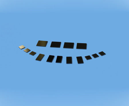
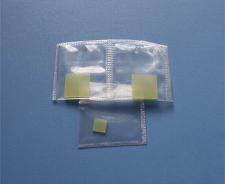
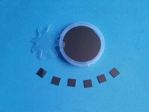
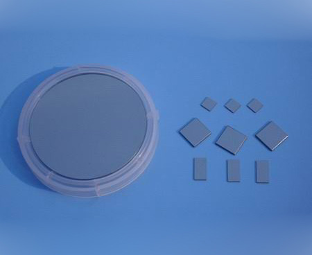
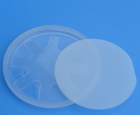
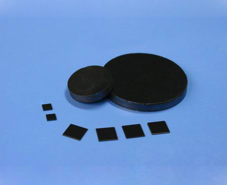
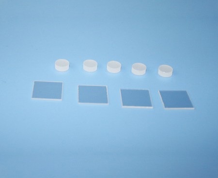
Indium arsenide, InAs substrate. InAs single crystal as a substrate can be use to grown InAsSb / In-AsPSb, InNAsSb and other heterojunction materials, Produced wavelength 2 ~ 14μm infrared light-emitting devices, InAs single crystal substrate can also be use to epitaxial growth a superlattice structure material AlGaSb, Produce mid-infrared quantum cascade laser.
Contact Us
- BIOTAIN CRYSTAL CO., LIMITED
- Tel: (+86) 1506 0796 451
- Fax: (+86) 0597 2212602
- Email: sales@crystal-material.com
- Work Time ( GMT +8 ):
- 9 AM ~ 6 PM, Monday to Friday
- Main office: A7, No. 501, Denggaoxi Road, Xipi street, Xinluo District, Longyan, Fujian, China
Products Category
- Substrate Materials
- Single crystal substrates
- Optical windows
- Conductive glass
- Ceramic substrates
- Single Crystals
- Sputtering Targets
- Compound Ceramic Target
- Alloy targets
- High purity Metal targets
- Evaporation material
- Oxides materials
- Fluorides materials
- Metal materials
- Nitride, Sulfide and Selenide
- High purity Nano powders