
BIOTAIN CRYSTAL > Substrate Materials > Single crystal substrates > Product Information > Next :GaSb substrate
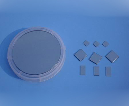
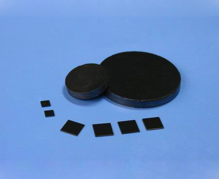
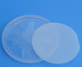
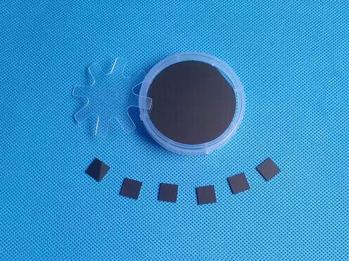
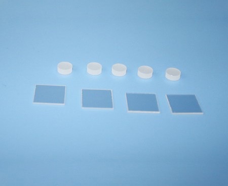
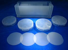
GaAs substrate
|
Standard Specification |
|||||||
| / |
Dopant
|
Conduction type
|
Carrier concentration
(cm-3) |
Dislocation density
(cm-2)
|
Growth method
|
Standard substrate
|
|
|
GaAs
|
Un-doped
|
Semi-insulating
|
/
|
< 5000 /cm2 Or <1000 /cm2 Or <500 /cm2 |
LEC
HB
VGF
|
Dia6"x0.65mm
Dia4"x0.6mm Dia3"x0.5mm
Dia2"x0.35mm
|
|
|
Si-doped
|
N-type
|
>5x10¹⁷
|
|||||
|
Cr-doped
|
Semi-insulating
|
/
|
|||||
|
Fe-doped
|
N-type
|
~2×10¹⁸
|
|||||
|
Zn-doped
|
P-type
|
>5×10¹⁷
|
|||||
|
Orientation
|
<100>
<100> with 2° off toward <111> <100> with 15° off toward <111> Orientation tolerance: ±0.5° |
||||||
|
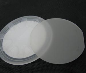
Standardd Size
|
25x25x0.5mm, 10x10x0.5mm, 10x5x0.5mm, 5x5x0.5mm
φ2"x0.35mm, φ3"x0.5mm, φ4"x0.6mm, φ6"x0.65mm
Special size and orientation are available upon requirements
|
||||||
|
Polishing
|
Single side polished or Double side polished
|
||||||
|
Surface roughness
|
Ra:<=5A (0.5nm)
|
||||||
|
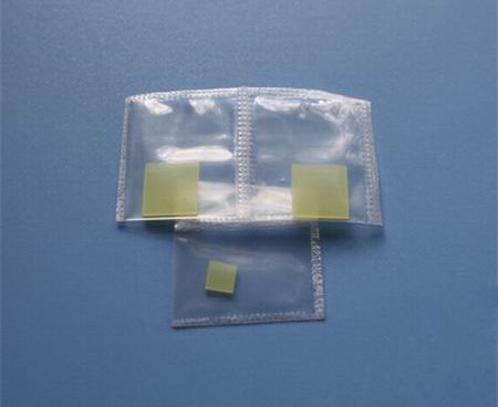
Package
|
class-100 clean bag,class-1000 clean room
|
||||||
Gallium arsenide (GaAs) crystal has good chemical stability, High hardness, resistance to harsh environment capability, It has a good permeability in 2μm-14μm spectral range, Widely used in thermal infrared imaging systems, high-power CO2 laser optical system and FLIR systems.
Contact Us
- BIOTAIN CRYSTAL CO., LIMITED
- Tel: (+86) 1506 0796 451
- Fax: (+86) 0597 2212602
- Email: sales@crystal-material.com
- Work Time ( GMT +8 ):
- 9 AM ~ 6 PM, Monday to Friday
- Main office: A7, No. 501, Denggaoxi Road, Xipi street, Xinluo District, Longyan, Fujian, China
Products Category
- Substrate Materials
- Single crystal substrates
- Optical windows
- Conductive glass
- Ceramic substrates
- Single Crystals
- Sputtering Targets
- Compound Ceramic Target
- Alloy targets
- High purity Metal targets
- Evaporation material
- Oxides materials
- Fluorides materials
- Metal materials
- Nitride, Sulfide and Selenide
- High purity Nano powders